NVIDIA Tesla V100: Last year also on PCI Express slots
The new NVIDIA parallel computing solution also announced for PCI Express systems: slightly smaller clock rates but reduced TDP.
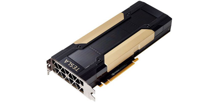
NVIDIA has officially announced, in conjunction with the International Supercomputing Conference (ISC), the new Tesla video card version intended for use in data-centers and based on traditional PCI Express design instead of the NVLINK interconnection developed by NVIDIA.
Of course, we are talking about the Tesla V100 card, the first based on next-generation Volta architecture and model that was announced by NVIDIA at the GTC conference in May. At that location, AMD had shown Tesla V100 in SXM2 package for direct installation on the compatible server motherboards, while the ISC announcement relates to the card version with a traditional 16x PCI Express connection.
This technical choice facilitates life for those who want to configure Tesla V100 card-based systems, as they can use almost all types of motherboards on the market, requiring only a PCI Express 16x slot. Between the two Tesla V100 card, slots slightly change some technical specifications, so much else was already done before with the two different versions of the Tesla P100 card based on Pascal’s previous generation architecture.
The Tesla V100 card on SXM2 connection has a GPU boost clock speed of up to 1.455 MHz; For the Tesla V100 card on PCI Express slot this data stops at approximately 1,370 MHz, so a slightly lower peak calculation power of 28 TFLOPS with half precision processing with 30 TFLOPS of the SXM2 card. Nothing changes for the remaining parameters, with 16 Gbytes of HBM2 video memory with 4,096 bit amplitude buses and 5,120 CUDA cores integrated into each GPU.
The lowest frequency of the Tesla V100 card slot for the PCI Express 16x slot justifies a lower TDP for this card: we move from the 300 Watt SXM2 model to 250 Watts of this proposal. In either case, cooling is completely passive, as the heat sink uses the air moved from the integrated fans inside the server where the card is housed.
Notice how the first and the most complex NVIDIA V100 chip of the next-generation Volta family is currently the largest GPU ever built. Based on 12 nanometer production technology, this solution has a total surface area of 815 millimeters square. The availability of this card is only scheduled for the end of the year, as does the rest of the SXM2 version announced by NVIDIA during May.